

Scanning Electron Microscope (SEM)
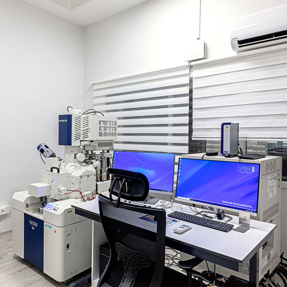
Scanning Electron Microscope (SEM)
SEM (HITACHI SU7000 Field Emission SEM)
Device Description
The electron microscope is used for imaging materials at the micro/nano scale and for determining the elemental and chemical compositions of materials.
Assoc. Prof. Dr. Sevde ALTUNTAŞ
LAB 102
- Acceleration voltage: 30 kV
- Point resolution: 0.8 nm (@15 kV), 0.9 nm (@1 kV)
- Sample stage tilt angle: -5~70°
- Detectors: UD (Upper Detector), MD (Middle Detector), LD (Lower Detector), UVD (Ultra Variable Pressure Detector)
- Variable Pressure (VP) mode
- EDX detector
- STEM detector
- Imaging of micro/nano structures
- Imaging of the structures of biological samples
- STEM imaging
- Point analysis of the elemental and chemical compositions of materials
- EDX mapping
